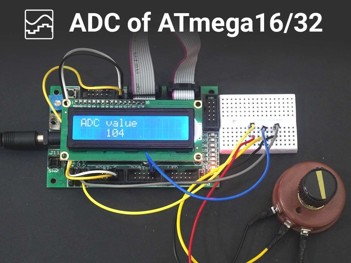
PIC18F4550 ADC
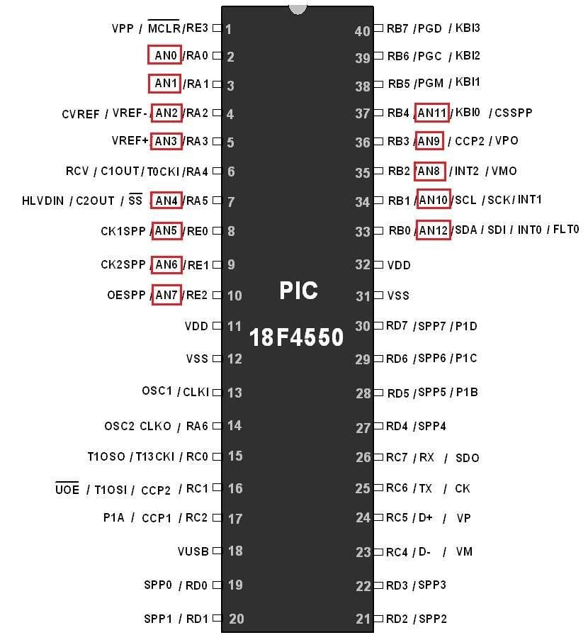
PIC18F4550 has a 10-bit internal ADC with 13 input channels.
Introduction Analog to Digital Converter
- When we interface sensors to the microcontroller, the output of the sensor many of the times is analog in nature. But microcontroller processes digital signals.
- Hence we use ADC in between sensors and microcontrollers. It converts an analog signal into digital and gives it to the microcontroller.
- There are a large number of applications of ADC like in a biometric application, Environment monitoring, Gas leakage detection, etc.
So now let’s see ADC in PIC18F4550.
- PIC18f4550 has inbuilt 10-bit 13 channel ADC.
- 13-channels of ADC are named as AN0-AN12. It means we can connect 13 different sensors at the same time.
- 10-bit ADC means:
- It will give digital count in the range of 0-1023 (2^10).
Digital Output value Calculation
- To keep things simple, let us consider that Vref is 5V,
For 0Vin digital o/p value = 0
For 5Vin digital o/p value = 1023 (10-bit)
For 2.5Vin digital o/p value = 512 (10-bit)
PIC18F4550 ADC Pins
ADC Registers of PIC18F4550
ADRESH (High byte) and ADRESL (Low byte) Registers are used in combination to store the converted data i.e. digital data. But the data is only 10-bit wide, so the remaining six bits are not used.
ADCON0: A/D Control Register 0
CHS3:CHS0: Analog Channel Select Bits
| CHS3:CHS0 | Channels | Channel Name |
| 0000 | Channel 0 | AN0 |
| 0001 | Channel 1 | AN1 |
| 0010 | Channel 2 | AN2 |
| 0011 | Channel 3 | AN3 |
| 0100 | Channel 4 | AN4 |
| 0101 | Channel 5 | AN5 |
| 0110 | Channel 6 | AN6 |
| 0111 | Channel 7 | AN7 |
| 1000 | Channel 8 | AN8 |
| 1001 | Channel 9 | AN9 |
| 1010 | Channel 10 | AN10 |
| 1011 | Channel 11 | AN11 |
| 1100 | Channel 12 | AN12 |
GO/DONE’: A/D Conversion Status Bit
When ADON=1
1= A/D conversion is in progress
0= A/D is idle
ADON: A/D Conversion Enable/ON bit
1= A/D conversion is ON (Start conversion).
0= A/D conversion is disabled.
ADCON1: A/D Control Register 1
VCFG1: Voltage Reference Configuration bit
1= Vref –
0= Vss
VCFG0: Voltage Reference Configuration bit
1= Vref +
0= Vdd
PCFG3:PCFG0: A/D Port Configuration Bits:
As the ADC pins in PIC18F4550 are multiplexed with many other functions. So these bits are used to de-multiplex them and use them as an analog input pin.
.jpg)
ADCON2: A/D Control Register 2
ADCS2:ADCS0: A/D clock conversion select bits:
These bits are used to assign a clock to ADC.
111= FRC Clock derived from A/D RC oscillator
110= FOSC/64
101= FOSC/16
100= FOSC/4
011= FRC Clock derived from A/D RC oscillator
010= FOSC/32
001= FOSC/8
000= FOSC/2
ADFM: A/D Result format select bit:
The 10-bit result will be placed in ADRESH (8-bit) and ADRESL (8-bit).
Consider 10-bit data as follows:

1 = Right Justified. However, the lower 8-bits are kept in ADRESL, and the remaining MSB side two bits kept in ADRESH. And remaining 6 bits (bit 2-7) of ADRESH filled with 0’s.

0 = Left Justified. However, the upper 8-bits are kept in ADRESH, and the remaining two lower bits are placed in ADRESL at bit 7-6 location. And the remaining 6 lower bits of ADRESL filled with 0’s.

ACQT2:ACQT0: A/D Acquisition Time Select Bits:
User can program acquisition time.
Following is the minimum wait time before the next acquisition can be started.
TAD = (A/D Acquisition Time)
000= 0 TAD. Default Acquisition Time for A-D conversion.
001= 2 TAD
010= 4 TAD
011= 6 TAD
100= 8 TAD
101= 12 TAD
110= 16 TAD
111= 20 TAD
Steps for Programming A/D Conversion
Initialization
- Configure ADCON1 Register to select Reference voltage using VCFG1: VCFG0 bits and also configure port pins which we require as an analog input using PCFG3: PCFG0 bits.
- Configure ADCON2 Register to select A/D result format, A/D clock, and acquisition time.
void ADC_Init()
{
    TRISA = 0xFF;	/* Set as input port */
    ADCON1 = 0x0E;	/* Ref vtg is VDD and Configure pin as analog pin */
    ADCON2 = 0x92;	/* Right Justified, 4Tad and Fosc/32. */
    ADRESH=0;		/* Flush ADC output Register */
    ADRESL=0;
}
A/D conversion and Read digital values
- Configure ADCON0 Register to select a channel that we require using CHS3: CHS0.
- Start A/D conversion by setting ADON bit and Go/done’ bit of ADCON0 Register.
- Wait for G0/done’ bit which is cleared when the conversion is completed.
- Then copy Digital data which is stored in ADRESH and ADRESL Register.
int ADC_Read(int channel)
{
    int digital;

    /* Channel 0 is selected i.e.(CHS3CHS2CHS1CHS0=0000) & ADC is disabled */
    ADCON0 =(ADCON0 & 0b11000011)|((channel<<2) & 0b00111100);

    ADCON0 |= ((1<<ADON)|(1<<GO));	/*Enable ADC and start conversion*/

    /* Wait for End of conversion i.e. Go/done'=0 conversion completed */
    while(ADCON0bits.GO_nDONE==1);

    digital = (ADRESH*256) | (ADRESL);	/*Combine 8-bit LSB and 2-bit MSB*/
    return(digital);
}
Application
- Here we are going to develop a short application using the internal ADC of PIC18f4550.
- In this, we will interface a 1K potentiometer which is used to vary the voltage.
- This varying voltage is applied to AN0 (channel 0) of ADC and displays this value on 16x2 LCD.
Interfacing Diagram
.JPG)
PIC18F4550 ADC Program
#include <stdio.h>
#include <string.h>
#include <stdlib.h>
#include <P18F4550.h>
#include "config_intosc.h"	/* Header File for Configuration bits */
#include "LCD_8bit_file.h"	/* Header File for LCD Functions */

void ADC_Init();
int ADC_Read(int);

#define vref 5.00		/* Reference Voltage is 5V*/
void main()
{
    char data[10];
    int digital;
    float voltage;
    OSCCON=0x72;		/*Set internal Osc. frequency to 8 MHz*/
    LCD_Init();			/*Initialize 16x2 LCD*/
    ADC_Init();			/*Initialize 10-bit ADC*/

    LCD_String_xy(1,1,"Voltage is...");

    while(1)
    {
        digital=ADC_Read(0);

	/*Convert digital value into analog voltage*/
        voltage= digital*((float)vref/(float)1023);

	/*It is used to convert integer value to ASCII string*/
        sprintf(data,"%.2f",voltage);

        strcat(data," V");	/*Concatenate result and unit to print*/
        LCD_String_xy(2,4,data);/*Send string data for printing*/
    }

}

void ADC_Init()
{
    TRISA = 0xff;		/*Set as input port*/
    ADCON1 = 0x0e;  		/*Ref vtg is VDD & Configure pin as analog pin*/
    ADCON2 = 0x92;  		/*Right Justified, 4Tad and Fosc/32. */
    ADRESH=0;  			/*Flush ADC output Register*/
    ADRESL=0;
}

int ADC_Read(int channel)
{
    int digital;
    ADCON0 =(ADCON0 & 0b11000011)|((channel<<2) & 0b00111100);

    /*channel 0 is selected i.e.(CHS3CHS2CHS1CHS0=0000)& ADC is disabled*/
    ADCON0 |= ((1<<ADON)|(1<<GO));/*Enable ADC and start conversion*/

    /*wait for End of conversion i.e. Go/done'=0 conversion completed*/
    while(ADCON0bits.GO_nDONE==1);

    digital = (ADRESH*256) | (ADRESL);/*Combine 8-bit LSB and 2-bit MSB*/
    return(digital);
}
Video
Components Used
Powered by
Downloads
Comments27
Join the discussion — share a question or tip.
- PR
Hi I have used code which u have created for ADC implementation for PIC18F4550 controller and it is working good. I need to implement three analog channels for displaying the values of voltage (input & output) as well as output current. Can you please suggest how I can initialize three channels simultaneously for the same.
- DN
Are you able to build the same project in the MPLAB X ?
- MI
Hi, This has helped me a great deal and works perfectly - thank you. Ho do you add an additional channel? Kind regards, Mike
- NA
there is no make executable error? can anybody help me please?
- PA
how to write the adc code using interrupt service routine.. plzz help..
- NN
Hello, can you give me the "config_intosc.h" header file for research?
- VI
Hi, I am very much interested to know ,how to use reference voltage using analog pins excluding VCC and GND
- BA
Pls I want to implement this project on PIC18f2550 , so how will the code be
- AN
This information is very useful and it helps me a lot because I am in starting of working with PIC Microcontrollers. Can any one please help me how can I measure AC voltage and AC current using PIC18f4550. Currently I have ACS712 current sensor which is working fine for DC loads but the code is not working for AC loads. How can I proceed further.
- AU
as per @Isteward answers it seems like he is using 1602a LCD . make sure your LCD connections with pic controller and your pic kit not using the same pins as your lcd ( as mentioned by @Isteward )
- VI
Replying to @authorized
Hello. Problem solved, thanks to everybody. It was effectivelly a problem of pins as per @lsteward comments, thanks to him. Now, I need to interface a HX711 load cell in serial mode, I beleive that I need to jump on your tutorial about UART, if not, please advise me the direction to take to interface it. Have a nice day and HAPPY NEW YEAR to everybody, health and prosperity to everybody
- AU
Replying to @Vinivini
@vinivini, Happy new year to you too. i think HX711 is not using UART communication instead it using serial data out and serial clock in pin to get data out with logic ( applying 25~27 positive clock pulses at the clock pin, data is shifted out on the data pin. ) something looks like: unsigned long ReadCount (void) { unsigned long Count; unsigned char i; data_pin=1; clock_pin=0; Count=0; while(data_pin); for (i=0;i<24;i++){ clock_pin=1; Count=Count<<1; clock_pin=0; if(data_pin) Count++; } clock_pin=1; Count=Count^0x800000; clock_pin=0; return(Count); } the returning count will be in 800000h (MIN) - 7FFFFFh (MAX). and this 24 bits of data is in 2’s complement format. hope you will find it right.
- VI
Replying to @Vinivini
Hi. Maybe I am a little bit stupid in this starting year, but I implemented your idea as below and it doesn't work at all. Some idea ? void main() { OSCCON=0x72; /* use internal oscillator with * MHz frequency */ TRISB = 0x00001000; /* define the I/O bits unsigned long ReadCount (); unsigned long Count; while(1) { Count = ReadCount (); } } unsigned long ReadCount () { ....and so on Where did I make a mistake.... mouahhhh.. Vincent
- AU
Replying to @Vinivini
i just give you logic in c. its not for tested or working as it is for pic. it need to be implemented with right clock frequency ( as mentioned for HX711 datasheet ) and write read/write sequence. you should make sure about these things.
- KA
very very thank you for this information...
- IS
Thanks for your input on this. I directly loaded hex with same result (second line of lcd not showing data) and I used the more simple LCD project provided and used this to try and solve my issue. It is possible I am missing some step in building. Here is how I build it. I download the provided project from your website to a separate location (say A) on my c drive. I then create a new standalone project in mplab x ide. I select PIC18f4550 and pickit3 and xc8 compiler and then save project with the same name as set in your download. I then copy the directory structure from location A over the directory structure created in mplab. I don’t change any configuration and I wire my circuit exactly as shown from your circuit. I also change pickit 3 to not supply power to circuit. if there is a more correct way to buil then let me know. When I continued my troubleshooting I did get a strange outcome. First of all I wired the pickit 3 as follows Pin 1 to mclr Pin 2 to Vdd Pin 3 to Vss Pin 4 to pic pin 40 (also used as output to lcd as per your circuit) Pin 5 to pic pin 39 (also used as output to lcd as per your circuit) I was not sure this would work but it certainly transfers the hex to pic without error. But here is the strange effect. I download the hex and the lcd 1602a shows nothing on line 1 and garbage in Line 2. I remove my external 5v power and reconnect the 5v supply and it shows ‘Hello’ in line 1 and blanks in line 2. I then remove the pickit 3 connections and then reconnect them and the two lines show correctly. I repeated this process even with the pickit3 not connected to my pc with the same behavior. I can only conclude from this that my lcd is working ok and my issue appears to be related to the connections from pickit3 to the pic. I created many PIC18f4550 projects with success. This is the first where I needed to have the pickit 3 and the pic share pin 39 and 40. If you use pickit3 to download the hex then could you let me know the connections you used and any other circuit modifications you needed to make? I really appreciate your help on this and thanks for your patience.
- DH
Hey before building the project you need to provide some directories, just entering the project folder path does not work. So here are the directories which you need to enter: 1. goto build options in project menu and click on project, 2. a new pop up will open like build options for your projects, 3. in directories tab the first one is: 1. Output Directories - create a new directory in it and select your project folder and click on apply, 2. Intermediary directory - create new directory and select mcc18 folder of mplab, 3. Include Search Path create new directory and select mcc18 folder in mcc18 folder select h folder of mplab, 4. Library Search Path - create new directory and select mcc18 folder in mcc18 folder select lib folder of mplab, 5. Linker Script Path - create new directory and select mcc18 folder in mcc18 folder select LKR folder of mplab Once you create all the directories and apply them then you need to click on OK and then your c file is good to go. I hope this helps. I didn't get any issues with the pickit3, so yeah the above steps just work fine with me.
- IS
Hi I am very impressed with the projects you have created. Thanks. I have completed the project above (PIC18f4550 ADC) but I cannot write to the 2nd line of the Lcd 16x2. The code initially did not compile until I included the following line #include “LCD_8bit.c” I am not sure if sure if the two issues are connected. Also I started to build the GPS Information.X and again I had to include the lcd and Usart c files as includes. Can you help me to resolve the 2nd line display issue?
- LO
@Isteward: Hi Isteward, It is working for me fine. There is no need to include LCD_8bit.c. 1. Test your LCD by directly loading .hex file into the controller which you can find in attachment. 2. Also you can try just LCD program provided in PIC18F4550 interfacing section to test your LCD. 3. If LCD is working properly then it may possible that you are missing some step while building project or we will dig out if it still not working with you. let me know about your problem is solved or not.